 |
Graphenea, Spain, announced on July 25, 2014 that together with Ritsumeikan University in Japan, the growth of GaN crystals on the silicon (100) surface was realized. The main point is to use graphene as an intermediate layer. The technology was developed by the R&D Institute of Science and Technology of Ritsumeikan University in Japan and the research laboratory of Yasushi and Yasushi of West Asia, the Massachusetts Institute of Technology (MIT), Seoul National University, and Dongguk University. Dongguk University) and Graphenea, Spain.
It is very difficult to directly grow GaN crystals with few defects on the silicon (100) surface, and there is almost no successful precedent. In the past, advances in practical use of GaN-on-Si technology have mainly focused on the growth of GaN crystals on the silicon (111) surface. One of the advantages of the GaN-on-Si technology is its ability to use existing silicon semiconductor fabrication facilities, but most semiconductor fabrication facilities target silicon (100) planes and GaN-on-on silicon (111) planes. Si technology, its scope of use is limited.
Under this circumstance, there have been cases where GaN crystal growth was successfully achieved after forming an intermediate layer on the Si(100) surface. Nagoya University is one of them. Professor Tian Tianhao’s research department of the Graduate School of Engineering of the University created a “metal layer†on the silicon (100) surface, and then succeeded in realizing the crystallization of GaN on the metal layer. Grow.
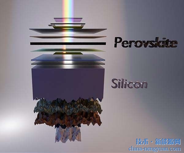
Graphene and others first formed graphene on the silicon (100) surface, and then realized GaN crystal growth on the (0001) surface on graphene. Detailed steps are as follows.
First, graphene is formed on a copper (Cu) foil by an ordinary chemical vapor deposition (CVD) method. It is then transferred to a silicon substrate. At this time, the Cu foil was removed by etching.
Then, GaN crystals were grown on graphene on the silicon substrate by RF-MBE (Radio-Frequency Molecular Beam Epitaxy). According to Graphenea, the RF-MBE method is a technology provided by Ritsumeikan University and plays an important role in crystal growth of GaN with high crystallinity.
When the grown GaN is detected by a scanning electron microscope (SEM) and a high resolution X-ray diffraction technique, the GaN crystal is shown to have a hexagonal symmetry and grows in the c-axis direction. In addition, the particle size is larger than that without graphene. Compared with GaN crystals grown on a sapphire substrate, the highest quality is achieved from the GaN crystals grown on the silicon (100) face despite the problem of alignment uniformity.
Incidentally, Fujioka’s research office at the University of Tokyo also announced the growth of GaN crystals on graphene (see our reports 1 and 2). However, Fujioka et al. are not silicon, but form GaN crystals on glass. Moreover, the RF-MBE method is not used, but the sputtering method is used. (Reporter: Nozawa Tetsuru, Nikkei Electronics)
38 Inch ABS Ceiling Fan
There are much more Ceiling Fan styles in our website,such as AC Motor Ball Style Ceiling Fan Light,Crystal Style Retractable Ceiling Fan,Iron Blades Ceiling Fan Without Light ,Solid Wood DC Ceiling Fan ,Real Wood Ceiling Fan with Light,and best Intelligent WIFI Ceiling Fan,ect.And there are more items are not showing on the website,please feel free to contact us directly for more information.
Small LED Ceiling Fans,White AC Ceiling Fan,Smart Ceiling Fan with Light,Ceiling Fan With Remote
JIANGMEN ESCLIGHTING TECHNOLOGY LIMITED , https://www.jmesclightingfan.com
