 |
Figure 1. Preparation of Cu2O single crystal films: XRDθ-2θ scan results of (a) Cu2O(111) and (b) Cu2O(110) thin films on ZnO template and RHEED monitoring results; (c) ZnO/Cu2O heterojunction prototypes Device schematic and IV test results; (d) XRD θ-2θ scans and RHEED monitoring results for Cu2O single crystal films on sapphire; (e) XRD scan results for single crystal Cu2O films on sapphire.

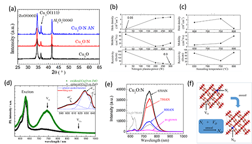
Figure 2. Cu2O optoelectronic performance control and defect studies: (a) XRD θ-2Î¸ï± scan results for nitrogen doped samples; (b) Electrical properties as a function of doping concentration and (c) Electrical annealing Results of temperature changes; (d) PL measurements at room temperature and fitting of exciton emission peaks with phonon-assisted models; (e) Room-temperature PL spectra of nitrogen-doped samples; (f) Impurity defects in nitrogen-doped samples Mechanism of action schematic.
Cuprous oxide (Cu2O) is an excellent semiconductor material. It has a direct gap of 2.1eV (590nm) and a high visible light absorption coefficient, plus it has the advantages of being non-toxic, inexpensive, and rich in raw materials. Has become an important material in the field of solar energy conversion and utilization research. The theory predicts that the efficiency of solar cells based on Cu2O can reach 20%. After the introduction of a suitable intermediate band by doping, the theoretical limit of the photoelectric conversion efficiency can be further increased to ~60%. At the same time, Cu2O has photocatalytic activity and can directly use visible light to catalyze the cracking of water to produce hydrogen.
Institute of Physics, Chinese Academy of Sciences/Beijing National Laboratory for Condensed Matter Physics (CCP) The Key Laboratory of Clean Energy Frontier Research Du Xiaolong’s research group has continued a series of studies on controlled growth, doping and defect control of Cu2O single crystal films. Some important progress has been made. Cu is in the middle valence state in Cu2O, which brings difficulties to the preparation of single-valent Cu2O. Mei Zengxia, Li Junqiang, Dr. Du Xiaolong, etc. achieved the oxidation process by systematically studying the oxidation kinetics of Cu film. The precise control suppresses the formation of metallic Cu or bivalent CuO clusters caused by underoxidation or overoxidation, and further develops the epitaxial growth process of Cu2O using molecular beam epitaxy in linings of ZnO, MgO, SrTiO3, etc. A high quality Cu2O single crystal thin film was prepared on the bottom. By adjusting the copper-enriched/enriched growth conditions, the intrinsic defect species and concentration in the film were regulated, strong exciton emission was observed at room temperature, and it was confirmed that copper vacancies (VCu) were the main factors affecting the exciton characteristics. However, the content of oxygen vacancies (VO) has little effect on exciton emission.
Doping is a necessary means to regulate the photoelectric properties of Cu2O to meet the application needs of the device. Recently, the team cooperated with Meng Qingbo, a researcher of E02 group, Ji Ailing, a research fellow of SF3 group, and Andrej Kuznetsov of the University of Oslo, Norway, to realize Cu2O through nitrogen doping technology. The electrical regulation, and systematically studied the dynamic behavior of impurities and defects in the Cu2O lattice. The incorporation of N atoms will occupy the O atom to form a substitutional atom, which will lead to an increase in the VO content in the film, and some N atoms will form an interstitial atom (Ni). Ni is a defect that has been neglected for a long time in the research. However, the team's research results prove that its interaction with other defects has an important influence on the photoelectric properties of Cu2O thin films. Under proper annealing conditions, Ni can migrate to the position of VO to fill this void, resulting in a decrease in VO and Ni and an increase in NO, resulting in a corresponding change in film properties. This work was published in Scientific Reports 4, 7240 (2014). Based on the understanding of the nitrogen doping mechanism, through the design of doping and annealing conditions, the photoelectric properties of Cu2O thin films can be greatly improved, laying a solid material foundation for their application in energy devices.
Two Bowls Handmade Kitchen Sink
Two Bowls Handmade Kitchen Sink,Small Double Sink Kitchen,Double Sink Kitchen,Double Bowl Sink
Zhongshanshi JiaBaoLu Kitchen And Bathroom Products Co., Ltd , https://www.gabalusink.com
