 |
Figure 1: Epitaxial growth of graphene on hexagonal boron nitride and characterization of AFM and Raman.

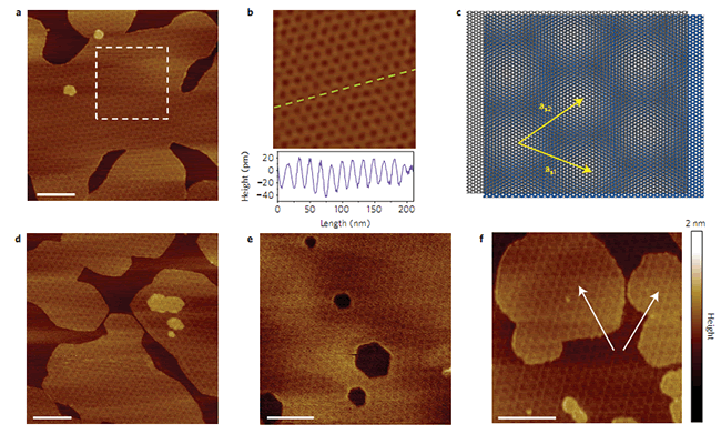
Figure 2: The AFM characterization can clearly observe the ~15nm graphene two-dimensional superlattice structure at various growth stages.

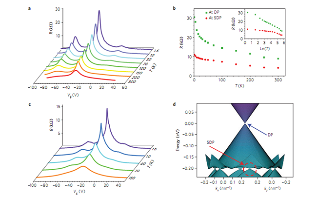
Figure 3: The graph of the electrical transport of graphene/hexagonal boron nitride as a function of temperature, the appearance of the superlattice Dirac point, and the corresponding band structure.

Figure 4: Quantum Hall transport curves at ~1.6K for monolayer and bilayer graphene.

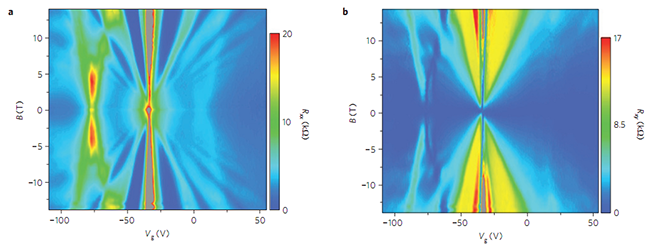
Figure 5: Radial resistance and Hall resistance of a single-layer graphene as a function of gate voltage and magnetic field.
Graphene has attracted much attention in condensed matter physics and materials science due to its unique linear energy dispersion relationship, high mobility, high thermal conductivity, and excellent mechanical properties. It is well-known that the properties of graphene are greatly affected by the substrate, and the commonly used silicon oxide substrate causes excessive carrier scattering and electro-acoustic interactions, which degrades the quality thereof.
Recent studies have found that hexagonal boron nitride can maximize the intrinsic physical properties of graphene due to its atomically flat surface, lack of dangling bonds, and weak doping effect. More importantly, graphene will form a two-dimensional superlattice structure on hexagonal boron nitride. Theoretical calculations show that this two-dimensional superlattice can regulate the energy band structure of graphene, form additional Dirac points, and provide an effective means for exploring a series of new physical phenomena, such as the Hofstadter Butterfly spectrum.
However, in the past, the transfer of graphene on the hexagonal boron nitride surface required the use of physical transfer technology, which would bring about processing and structural uncertainty. For example, graphene and boron nitride have a lattice mismatch of 1.7%, and the different stacks produce different superlattice cycles. Different superlattices will have different modulation behaviors for the graphene band, and the size of the open energy gap will also be different.
In addition, the physical transfer technology will also cause structural inhomogeneity, interface pollution and other issues. Therefore, how to control the stacking method of graphene on Hexagonal Boron Nitride, so that the periodicity of the two-dimensional superlattice is fixed, large-scale uniform, and high-quality pollution-free is a very challenging subject.
Recently, Institute of Physics of the Chinese Academy of Sciences/Beijing National Laboratory for Condensed Matter Physics (CIC) Nano physics and devices laboratory Zhang Guangyu, Shi Dongxia fellow, doctoral student Yang Wei et al. and Fudan University Professor Zhang Yuanbo, PhD student Chen Guorui, and Beijing Institute of Technology Yao Yugui Professors and Ph.D. Liu Xie and others collaborated on the work of epitaxially growing graphene on hexagonal boron nitride substrates and measuring the electrical transport properties of related superlattices. They are based on the previous graphene direct growth technology (Nano Res. 2011, 4, 315; Small 2012, 8, 1429; Nano Res. 2012, 5, 258), using methane as the gas source, enhanced by remote plasma The vapor phase epitaxy technology has realized the controllable van der Waals epitaxy of graphene on the hexagonal boron nitride inert substrate for the first time in the world.
This epitaxial graphene has a large area (limited only by the size of the substrate), single crystal, high quality (maximum carrier mobility of 20,000 cm2V-1s-1), controllable number of layers (1 to 3 layers), etc. advantage. The atomic force microscope was used to directly observe the lattice stacking modes of epitaxial graphene and boron nitride substrates with zero corners, and the lattice mismatch resulted in the emergence of a triangular moire pattern, thereby forming a two-dimensional super-crystal with a period of about 15 nanometers. Lattice structure.
This superlattice structure will modify the energy band of graphene, forming a new Dirac point at point M in the superlattice Brillouin zone. The results of electrical transport measurements show that there will be additional minimum conductance peaks arising from two-dimensional superlattice structures on both sides of the graphene intrinsic Dirac point, corresponding to electron and hole-supported superlattice Dirac points. Quantum Hall measurements were used to observe the half-integer quantum Hall effect of Dirac fermions for single-layer graphene and the octal degeneracy near the double-layer graphene Dirac point.
In addition, they also performed two-dimensional spectral studies with carrier concentration and magnetic field changes on the single-layer graphene radial resistance and Hall resistance. The corresponding transport properties were observed near the superlattice Dirac point, and observations were made. The super-crystal lattice with a degree of degeneracy of two. These results provide new methods and ideas for the epitaxial growth of graphene and the physical study of two-dimensional superlattices.
The related results were published in Nature Materials (2013, 12, 792).
This work was supported by the National Natural Science Foundation of China, the Ministry of Science and Technology, and the Chinese Academy of Sciences.
Pvb Film-Automotive,Pvb Interlayer Glass,Pvb Film Glass,Sgp Glass Interlayer
HUAKAI FENGSHI TECHNOLOGY (CHONGQING) CO., LTD. , https://www.cqhkpvb.com
